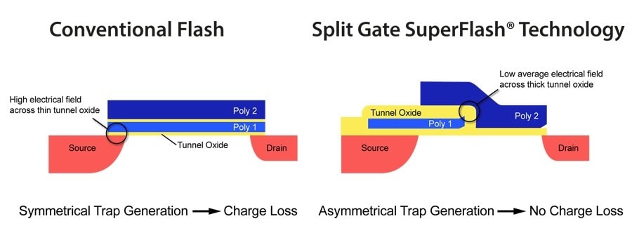
SuperFlash® technology is an innovative and versatile type of NOR Flash memory that utilizes a proprietary split-gate cell architecture to provide superior performance, data retention and reliability over conventional stacked gate Flash. Watch our SuperFlash Flash Memory Technology Advantages webinar to learn how the SuperFlash cell operates differently from a conventional Flash cell.
SuperFlash® Flash Memory Technology Advantages Webinar
Using a transistor-level memory cell description, this video explains the technical details behind SuperFlash memory's advantages over conventional NOR Flash memory. Better endurance, lower cell power, and 1000x better erase times are justified by comparing how the Flash and SuperFlash memory cells function differently.

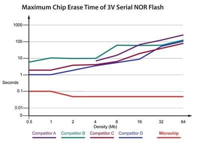
Industry's Fastest Erase Times
The unique split-gate cell design allows products with SuperFlash technology to provide the fastest sector, block and chip erase times available. While a typical 64 Mb Flash can take as long as 100 seconds to perform a full chip erase, the equivalent products with SuperFlash technology can complete the same operation in less than 100 ms.
As shown in Figure1, chip erase times become more significant as the density increases in competing devices. With SuperFlash technology, the chip erase remains extremely fast regardless of density.
Over-erase is a condition that affects traditional stacked gate Flash. An over-erased cell creates a leakage current path between the drain and floating gate, which can result in read failures. To combat this effect, stacked gate Flash requires multiple erase pulses, soft-programming and erase verification cycles to ensure a tight threshold voltage window of the Flash cell. Over-erase and the resulting cell leakage does not affect the split gate cell design of SuperFlash technology because the floating gate is isolated from the drain. Therefore, the additional soft-program and erase verify steps during cell erase are not required with SuperFlash technology. The result is a Flash memory that can perform a full chip erase up to 1,000 times faster than typical Flash.
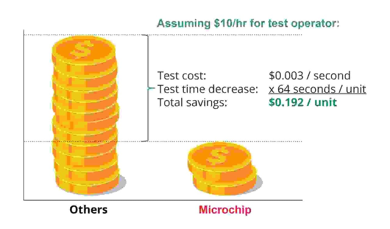
Faster Erase Times Save You Money
Your factories may be wasting valuable time testing Flash memory. SuperFlash memory drastically improves manufacturing throughput, saving test costs and avoiding the investment in additional test equipment to meet your customers’ demand. Stacked gate Flash requires minutes per board whereas SuperFlash only needs seconds. Don’t get caught off guard by this hidden product cost.
We have created an interactive savings calculator to show you what your annual savings might be if you choose SuperFlash technology. Give it a try.
High Reliability and Data Retention
Serial NOR Flash Memory (SPI, Quad SPI/QSPI) Products by Density
Parallel NOR Flash Memory Products by Density
Ready to Use SuperFlash Technology?
Serial SuperFlash® Kit 2
Part Number: AC243008
The Serial SuperFlash Kit 2 contains three serial Flash daughter boards that are designed to interface with the mikroBUS™ connector on the Explorer 16/32 Develoment Board.
SQI SuperFlash Kit 1
Part Number: AC243009
The SQI SuperFlash Kit 1 contains three serial Flash daughter boards that are designed to interface with the mikroBUS connector on the Explorer 16/32 Develoment Board.
Parallel SuperFlash Kit 1
Part Number: AC243006-1
This evaluation kit contains two parallel Flash PICtail™ Plus Daughter Boards that are designed to interface with the PICtail Plus connector on the Explorer 16 Development Board.