Our multiple-output and highly flexible quartz- and MEMS-based PureSilicon™ oscillators are available in a variety of industry-standard footprints to meet the requirements of your low-power or low-jitter applications. Use our Clockworks® Configurator and Sampling Tool to easily customize your oscillator to any combination of frequency, temperature, ppm and package size to suit the requirements of your application and then order samples from within the tool. You can also use our TimeFlash tool to customize and configure our MEMS oscillators. Please email us at tcg_help@microchip.com for more information.

Standard Oscillators (XOs)
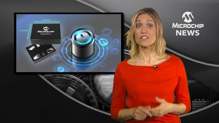
Our standard XOs are MEMS and quartz crystal-based oscillators. Offering low power and low jitter, these oscillators come in packages as small as 1.6 mm × 1.2 mm with frequency stability of 10 ppm to 100 ppm.

Voltage-Controlled Crystal Oscillators (VCXOs)
We designed these frequency-adjustable oscillators for phase locked loops, jitter cleaning and applications that require frequency tuning.

Temperature-Compensated Crystal Oscillators (TCXOs)
These small, low-power ASIC- and thermistor-compensated oscillators offer great stability, phase noise and g-sensitivity.

Voltage-Controlled SAW Oscillators (VCSOs)
Explore our high-frequency, tunable, ultra-low-jitter, rugged Surface Acoustic Wave (SAW) oscillators.

Oven-Controlled Crystal Oscillators (OCXOs)
Our OCXOs are temperature-controlled oscillators with optimal frequency, temperature, aging, phase noise and short-term stability (ADEV).

GNSS/PPS-Disciplined Oscillators (GNSS-DOs)
These oscillators are compact, multi-channel oscillator modules with exceptional holdover for positioning, navigation and timing applications.

Defense Oscillators
We designed these oscillators for high performance in harsh environments, such as shock and vibration, and wide or rapidly changing temperatures.

Space and High-Reliability Oscillators
Space applications need products with the highest reliability available for mission-critical platforms. Our oscillators meet screening and radiation requirements for Low Earth Orbit (LEO) and deep space environments.

Automotive Oscillators
We designed these AEC-Q100 qualified oscillators for high reliability, tolerance to shock and vibrations and automotive Grade 1 temperatures of −40 to +125°C.

PCIe® Oscillators
Our PCIe Gen 1/2/3/4/5/6-compliant MEMS and quartz oscillators are available in small package sizes with functionality across a wide range of temperatures.

5G Oscillators
These oscillators have best-in-class phase noise, stability, operating temperature and performance for leading-edge 5G designs.

Industrial Oscillators
We designed these oscillators specifically for high-temperature, shock, vibration, down hole, ocean bottom seismic, test and measurement, factory automation, industrial printers and medical applications.
Customize Your Oscillator with ClockWorks® Configurator
With just a few clicks, you can program your devices to any combination of frequency, temperature, ppm and package size to meet your specific application’s requirements. You can also use this tool to download customized data sheets and order custom samples with a 48-hour turnaround.
Need Some Help?
We are here to support you. Contact our Client Success Team to get assistance with your design.

- Application Notes
- Brochures
- White Papers
- FAQs
|
Title
|
|
|---|---|
| Quartz Crystals and Microchip ICs | Download |
| PAN1001281 - How to Measure Spread Spectrum Modulation - PAN1001281 - How to Measure Spread Spectrum Modulation | Download |
| PAN0905081 - PL611-01-F93 Power Supply Decoupling | Download |
| AN2477 - Microchip MEMS Oscillator and Clock Products for Automotive Applications | Download |
| Microchip’s Clock Devices Compliance with PCIe 4.0 | Download |
| Differential Clock Translation | Download |
| Jitter Blocker | Download |
| AN2399 - MEMS Oscillators Offer Immunity to EMI | Download |
| PicoPLL /PL611 Bluetooth Application Note | Download |
| PL671 Spread Spectrum Modulation | Download |
| AN2340 - Immunity of MEMS Oscillators to Mechanical Stresses - Immunity of MEMS Oscillators to Mechanical Stresses | Download |
| ANTC203 - ANTC203 - PCI Express ? Signal Integrity and EMI | Download |
| AN5225 - Reference Clocks for RT PolarFire® (Radiation Tolerant PolarFire) Transceiver | Download |
| AN3604 - Pre-Configured Clock Generator Part Numbers for Switchtec and Data Center Applications | Download |
| AN4287 - Oscillator Groups and Classifications | Download |
| Optimizing the OX-601/OX-502 Performance | Download |
| AN3467 - Crystals and Oscillators for Next Generation Timing Solutions | Download |
|
Title
|
|
|---|---|
| Oscillators - MEMS and Crystal Solutions Brochure | Download |
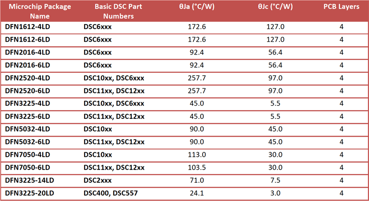
What are the Junction to Ambient (Theta JA) and Junction to Case (Theta JC) thermal resistance for the MEMS products?
Can a MEMS device select among different frequencies for a given output clock?
Is it possible to change the programmed output frequency?
What is the logic level for the input frequency select pins?
Are there MEMS devices that can generate two clock outputs from the same device?
How does the phase noise change with the carrier frequency?
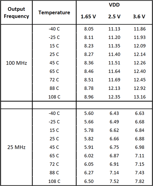
Does the supply current increase with the voltage supply and the clock frequency?
In addition to bypass capacitors, do you recommend using ferrite beads on the power supply (VDD)?
Can the MEMS devices latch up?
What is the difference between start-up time and enable time and how are they measured?
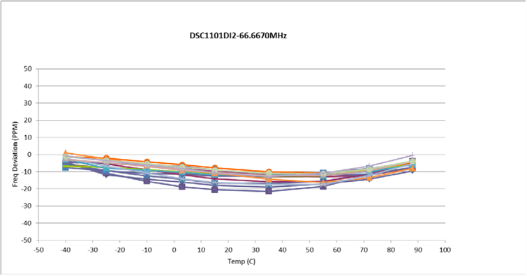
What is the frequency stability behavior over the temperature range?
Can the soldering process affect the frequency stability?
Can the MEMS oscillators/clocks work in a high-pressure environment, in particular up to 700 psi and surviving at 1,700 psi?
PCIe Overview
This 5-minute video provides the viewer with the fundamental concepts related to PCIe; it is the first video in a series that focuses primarily on the clocks and timing issues related to PCIe, and it also provides a basic understanding with which to explore further PCIe topics.
Intended Audience:
Anyone interested in an easy-to-understand high-level introduction to PCIe. No prior knowledge of PCIe is assumed.
What topics are covered?
1. Point-to-Point bus
2. Bi-directional bus
3. Scalability of data rates
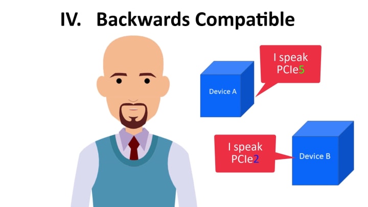
4. Backwards compatibility
5. Wide adoption across many markets
PCIe QuickLearn Video Series | Video #1 - PCIe Overview
Video #1 - PCIe® Overview
This 5-minute video covers the fundamental concepts related to PCIe. It is the first video in a series that focuses primarily on the clocks and timing issues related to PCIe. It also provides a basic understanding with which to explore further PCIe topics.
Intended Audience:
Anyone interested in an easy-to-understand high-level introduction to PCIe. No prior knowledge of PCIe is assumed.
What topics are covered?
- Point-to-Point bus
- Bi-directional bus
- Scalability of data rates
- Backwards compatibility
- Wide adoption across many markets
Cut Board Space by up to 80% on Timing Components
Cut Board Space by up to 80% on Timing Components
Learn how our small multi-ouput MEMS clock generators can reduce timing component board space by up to 80% in your design.
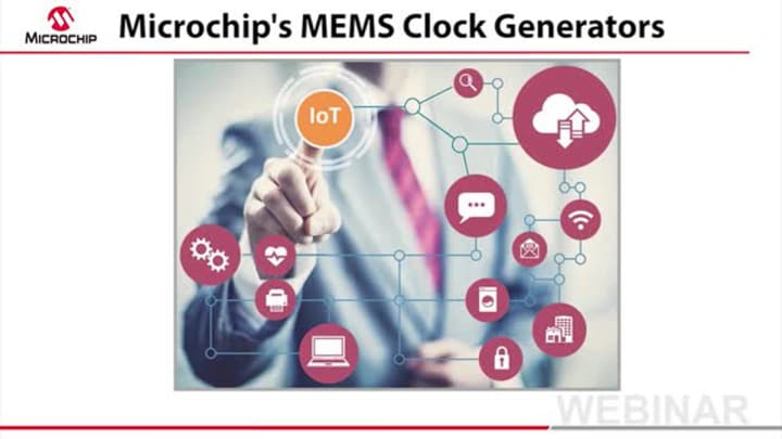
Microchip's MEMS Clock Generators Webinar
Microchip's MEMS Clock Generators Webinar
Can programmable MEMS-based clock generators make a significant difference in your Internet of Things or other connected design? Watch this video to learn how they offer accurate timing while simplifying your design and reducing the overall system bill-of-materials.
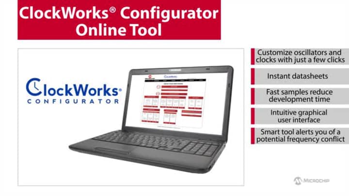
ClockWorks® Configurator Online Tool
ClockWorks® Configurator Online Tool
This video walks you through the features of ClockWorks® Configurator Online Tool and shows you how to customize oscillators and clock generators. With this easy-to-use tool, you can receive dynamic data sheets and samples within a few days.
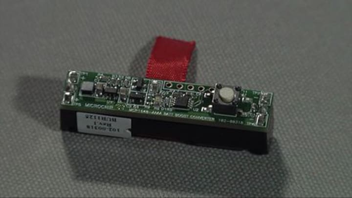
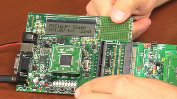
Single AAAA Battery Reference Design for Low Power PIC® MCUs
Single AAAA Battery Reference Design for Low-Power PIC® MCUs
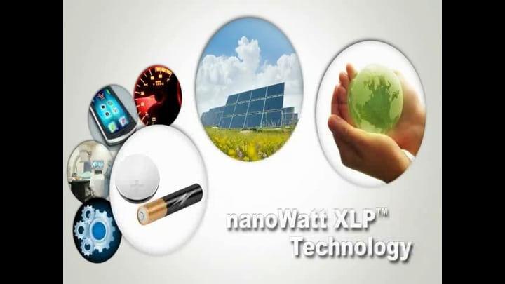
Learn how to power low-power microcontrollers with a single battery using voltage boost converters. As more electronic applications require low power or battery power, energy conservation becomes paramount. Today's applications must consume little power, and in extreme cases, last for up to 15–20 years, while running from a single battery. To enable applications like these, products with our nanoWatt XLP technology offer the industry's lowest currents for run and sleep, where extreme-low-power applications spend 90–99% of their time.
Benefits of nanoWatt XLP technology:
- Sleep currents below 20 nA
- Brown-out Reset (BOR) down to 45 nA
- Watchdog Timer (WDT) down to 220 nA
- Real-time Clock/Calendar (RTCC) down to 470 nA
- Run currents down to 50 μA/MHz
- Full analog and self-write capability down to 1.8V
Low Power MCU Comparision: nanoWatt XLP Vs. MSP430
Low Power MCU Comparision: nanoWatt XLP vs. MSP430
Three of nanoWatt XLP technology's key advantages are sleep currents down to 20 nA, Real-Time Clock currents down to 500 nA, and Watchdog Timer currents down to 400 nA. The vast majority of low-power applications require one or more of these features.
nanoWatt XLP technology combines all three in a comprehensive portfolio of devices. Whether your design requires extended battery life, sealed batteries or the integration of energy harvesting, our 8- and 16-bit PIC® MCUs with nanoWatt XLP technology are excellent options when your product needs to operate longer using less power or require fewer battery changes.
More Low Power MCU Comparisons: nanoWatt XLP Vs. MSP430
More Low-Power MCU Comparisons: nanoWatt XLP vs. MSP430
Three of nanoWatt XLP technology's key advantages are sleep currents down to 20 nA, Real-Time Clock currents down to 500 nA, and Watchdog Timer currents down to 400 nA. The vast majority of low-power applications require one or more of these features.
nanoWatt XLP technology combines all three in a comprehensive portfolio of devices. Whether your design requires extended battery life, sealed batteries or the integration of energy harvesting, our 8- and 16-bit PIC® MCUs with nanoWatt XLP technology are excellent options when your product needs to operate longer using less power or require fewer battery changes.
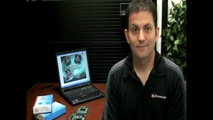
The World's Lowest Power in Sleep MCU: nanoWatt XLP from Microchip
The World's Lowest Power in Sleep MCU: nanoWatt XLP from Microchip
Three of nanoWatt XLP technology's key advantages are sleep currents down to 20 nA, Real-Time Clock currents down to 500 nA, and Watchdog Timer currents down to 400 nA. The vast majority of low-power applications require one or more of these features.
nanoWatt XLP technology combines all three in a comprehensive portfolio of devices. Whether your design requires extended battery life, sealed batteries or the integration of energy harvesting, our 8- and 16-bit PIC® MCUs with nanoWatt XLP technology are excellent options when your product needs to operate longer using less power or require fewer battery changes.
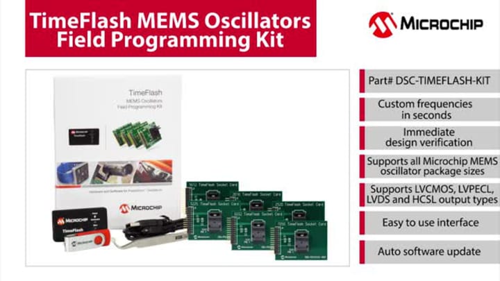
TimeFlash MEMS Oscillators Field Programming Kit
TimeFlash MEMS Oscillators Field Programming Kit
This video provides a quick demonstration of the TimeFlash MEMS Oscillators Field Programming Kit that allows you to program MEMS oscillators instantly to any frequency, anywhere. This kit supports all of our MEMS oscillator package sizes and is designed to enable rapid prototyping and testing.
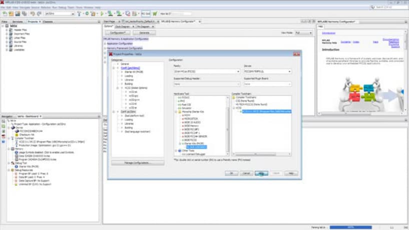
Application Migration Using MPLAB® Harmony
Application Migration Using MPLAB® Harmony
This video demonstrates how MPLAB® Harmony can enable application migration in three easy steps.
- Create new configurations with the same project.
- Choose the board support package for the new graphical display and clock settings for the new microcontroller.
- Configure the drivers and application libraries for the application.
The award-winning MPLAB Harmony framework with its configurator can enable application migration across boards with different microcontrollers, displays and graphics controller options without writing a single line of code to save time and resources.