Log in to myMicrochip to access tools and benefits. Sign up in just one minute.
Live Chat
Need Help?
Privacy Policy {"Stage_EswLiveAgentDevName":"EmbeddedServiceLiveAgent_Parent04I2f0000004CVTEA2_18385bcda98","Stage_SalesforceOrgId":"00D2f0000001OfB","Agent_Available_Header":"No problem. Chat with our engineering experts or schedule a call that's convenient for you.","Prod_SalesforceOrgId":"00Do0000000KAkK","Stage_SalesForcePath":"https://microchip--chipbot.sandbox.my.salesforce.com","Prod_EswLiveAgentDevName":"EmbeddedServiceLiveAgent_Parent04I3l000000CaZuEAK_184c4646b8d","Prod_BaseLiveAgentContentURL":"https://c.la4-c3-ph2.salesforceliveagent.com/content","Stage_ButtonId":"5732f0000008PHf","Prod_BaseLiveAgentURL":"https://d.la4-c3-ph2.salesforceliveagent.com/chat","Prod_ButtonId":"5733l000000Gonb","Stage_BaseLiveAgentURL":"https://d.la3-c1cs-ia2.salesforceliveagent.com/chat","Stage_JsUrl":"https://microchip--chipbot.sandbox.my.salesforce.com/embeddedservice/5.0/esw.min.js","Agent_Unavailable_Header":"An agent is not available to chat right now however please feel free to schedule a call with one of our team members.","Prod_SalesForceLAPath":"https://microchip.secure.force.com/mDirectLA","Prod_SalesForcePath":"https://microchip.my.salesforce.com","Stage_SalesForceLAPath":"https://microchip--chipbot.sandbox.my.salesforce-sites.com/mDirectLA","Stage_DeploymentId":"5722f0000008OpU","Service_Force_Url":"https://service.force.com","Prod_DeploymentId":"5723l000000GoUh","Schedule_Call_Url":"https://microchip.my.site.com/schedulemeetingportal/s/","Stage_BaseLiveAgentContentURL":"https://c.la3-c1cs-ia2.salesforceliveagent.com/content","Prod_JsUrl":"https://microchip.my.salesforce.com/embeddedservice/5.0/esw.min.js"}
Our Solutions
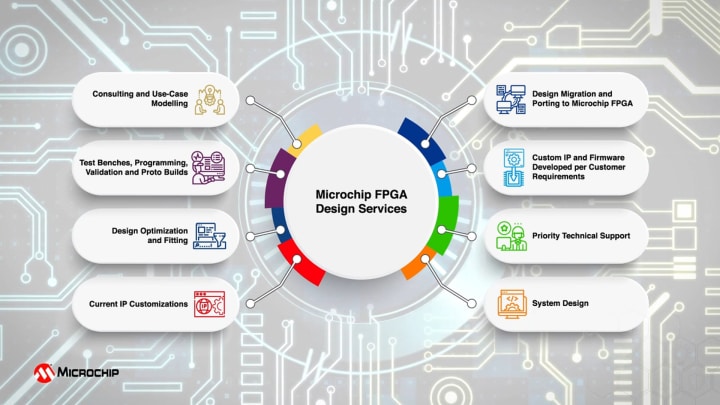
Reduce Risks and Costs and Fast-Track Your FPGA Design in Three Easy Steps
- Talk to us to help us understand your design requirements.
- Work with us to craft and sign a Statement of Work (SoW).
- Perform periodic reviews as we develop and test your design.
Learn More About FPGA Design Services